

Welcome to- Circuit Engineer
Paul Eisle developed the principal PCB in 1936. Be that
as it may, it got mainstream just during the 1950s when the US military began
utilizing the innovation in bomb detonators. Today, PCB Reverse Engineering
Circuit Boards are a fundamental piece of practically all hardware, similar to
vehicles, cell phones, PCs and then some.
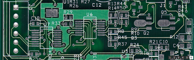
How Is A Reverse engineering
circuit board Manufactured?
To make a custom PCB, first the electronic chart of the necessary circuit is readied utilizing Computer Aided Design (CAD) programming. After that the PCB model is created utilizing Computer Aided Manufacturing Software innovation.
The normal materials utilized for assembling PCBs are:
FR4, FR4 High Temperature, Polyimide, GeTek, Rogers, Arlon, Nelco, Alumina,
Ceramic, Bakelite, FR1, CEM1, and CEM5. The size and thickness of the board
relies on the prerequisites of the circuit. The substrate is covered with a
layer of copper. At that point, utilizing photosensitive covering, the circuit
chart is imprinted on the board. The undesired copper is scratched out from the
board to shape copper "tracks", called follows. This cycle is known
as Photoengraving. There are two other regular strategies utilized for creating
associating follows. PCB processing is a mechanical framework where undesired
copper is taken out with CNC machines. Another interaction is Silk-Screen
printing, where exceptional ink that is draw safe is utilized to cover the
zones where the copper follows must be made.

When the board is prepared with copper follows,
openings are bored into the board to collect leaded electrical and electronic
segments. For penetrating, uncommon Tungsten Carbide boring tools or laser is
utilized. The openings made are loaded up with empty bolts or covered through
utilizing an electroplating cycle, subsequently framing an electrical
association among the different layers. The following stage is covering of the
whole board, aside from openings and cushions, with veiling material. Materials
ordinarily utilized for this intention are: lead bind, lead free weld, OSP
(Entek), profound/hard gold (electrolytic nickel gold), drenching gold
(electroless nickel gold - ENIG), wire bondable gold (99.99% unadulterated
gold), submersion silver, streak gold, inundation tin (white tin), carbon ink,
and SN 100CL, a combination of tin, copper, and nickel. The last advance is
screen-printing, where the legend and text are imprinted on the PCB.
Testing Of Reverse engineering PC board
Prior to gathering of parts or conveyance of Printed
Circuit Boards, the board ought to be tried to locate any potential
"shorts" and "opens" that could prompt a non-working board.
A "short" shows the presence of an undesired association and an
"open" demonstrates that two focuses that ought to have been
associated are detached. All such mistakes ought to be fixed before PCB get
together. It is essential to take note of that not all PCB Manufacturing shops
test the loads up prior to transportation, it is now and then thought to be an
additional expense yet a crucial one to give a completely working board prior
to adding segments.
PCB Assembly
When the board is prepared, parts are amassed and added
to the surface according to the circuit chart. A portion of the basic gathering
methods utilized are surface-mount development and through-opening development.
In some cases, a mix of these two strategies is likewise utilized for get
together.
Kinds of Clone PCB Board
Single Sided Board
This is the most un-complex of the Circuit board
cloning, since there is just a solitary layer of substrate. Every
electrical part and segments are fixed on one side and copper follows are on
the opposite side.
Twofold Sided Board
This is the most well-known kind of board, where parts
and segments are appended to the two sides of the substrate. In such cases,
twofold sided PCBs that have associating follows on both the sides are
utilized. Twofold sided Printed Circuit Boards generally use through-opening
development for gathering of parts.
Multi Layered Board
Multi layered PCB comprises of a few layers of
substrate isolated by protection. Most regular multilayer sheets are: four
layers, six layers, eight layers, and 10 layers. Nonetheless, the absolute
number of layers that can be fabricated can surpass more than 42 layers. These
sorts of sheets are utilized in very unpredictable electronic circuits.
Visit for more information- https://www.circuitengineer.com/

0 Comments